Understanding Lithography Machines in Modern Chip Production
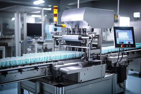
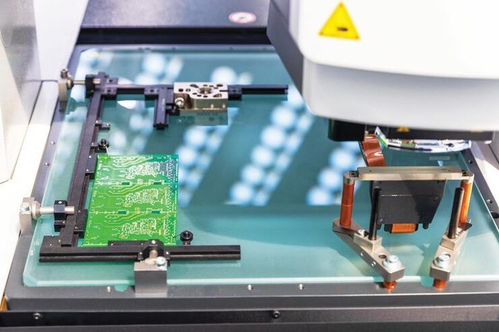
Lithography machines are among the most important technologies used in modern chip production. These systems help manufacturers create the tiny circuit patterns found inside processors, memory chips, sensors, and many other electronic components. In simple terms, a lithography machine works like an extremely precise printing system that transfers microscopic designs onto semiconductor materials. Those patterns eventually become the electrical pathways that allow electronic devices to process information, store data, and perform complex tasks. Without lithography systems, modern digital devices such as smartphones, laptops, industrial equipment, and connected appliances would not function at the level people expect today.
The comparison between different lithography machines matters globally because demand for advanced electronics continues to grow across industries. According to global industry research, semiconductor production has become one of the most strategically important manufacturing sectors due to increasing use of artificial intelligence, cloud computing, automation, electric transportation systems, and smart consumer products. Manufacturers are under pressure to create smaller, faster, and more energy-efficient chips while maintaining production quality and operational efficiency. As a result, understanding how lithography technologies differ has become increasingly relevant for engineers, researchers, technology investors, students, and businesses involved in electronics manufacturing.
The real-world impact of lithography machines extends far beyond chip factories. Faster medical devices, more reliable communication systems, efficient industrial automation, and improved digital infrastructure all depend on semiconductor innovation. Even people with no direct connection to manufacturing are affected by advancements in chip production because nearly every modern service relies on electronic processing systems in some form. Understanding how lithography technologies work and where they are evolving helps explain why chip manufacturing continues to shape global technological progress. This also leads naturally into understanding who is most affected by these developments and the practical problems these machines help solve.
Who it affects and problems it solves
Lithography machines affect a broad international audience because semiconductor technology supports many professional and personal activities. Engineers and chip designers depend on these systems to create increasingly compact electronic circuits. Manufacturers rely on lithography equipment to improve production precision and reduce defects during fabrication. Businesses involved in cloud infrastructure, robotics, medical technology, transportation systems, and telecommunications are also influenced because semiconductor performance directly impacts product reliability and efficiency. Students and researchers studying electronics or advanced manufacturing increasingly encounter lithography concepts as part of technical education and innovation programs.
Without clarity on lithography technologies, organizations often struggle to understand why chip manufacturing costs vary so widely between production methods. Some companies may invest in systems that do not align with their production goals, while others underestimate the operational complexity involved in advanced semiconductor fabrication. Different lithography approaches offer trade-offs between precision, production speed, energy consumption, scalability, and maintenance requirements. Comparing these factors helps decision-makers identify which systems are more suitable for mature manufacturing processes and which are better designed for advanced chip architectures.
A common challenge seen globally involves balancing performance expectations with manufacturing efficiency. For example, a company developing advanced processors for artificial intelligence may require extremely precise lithography systems capable of producing very small circuit structures. Meanwhile, manufacturers producing standard industrial chips may prioritize stability, cost efficiency, and long production lifecycles over maximum miniaturization. Many organizations make the mistake of assuming the most advanced lithography machine is automatically the best option for every application, even when simpler systems may provide better operational value. Understanding these differences creates a stronger foundation for evaluating recent industry developments and technological shifts.
Recent updates
Over the past year, semiconductor manufacturers have continued increasing investment in advanced lithography technologies to support growing demand for high-performance computing systems. Industry reports indicate that companies are focusing heavily on improving production yields while reducing energy consumption during fabrication. Greater attention is also being placed on manufacturing stability because small variations in chip production can significantly affect performance and reliability.
In early 2025, industry observers noted stronger collaboration between semiconductor equipment suppliers and chip designers. Rather than treating manufacturing equipment and chip architecture as separate processes, many organizations are now developing integrated strategies that optimize both design and fabrication simultaneously. This approach helps manufacturers improve efficiency while supporting increasingly complex chip structures.
Another major trend involves the expansion of automation within lithography operations. Manufacturers are using advanced monitoring systems, predictive maintenance tools, and machine learning technologies to identify potential production issues earlier in the fabrication process. According to global industry analysis, these improvements are helping reduce waste while increasing consistency across large-scale semiconductor manufacturing facilities.
Sustainability has also become a more visible topic across the semiconductor sector during the past 12 months. Many manufacturers are evaluating how lithography systems consume energy, water, and specialized materials throughout production cycles. As environmental expectations continue evolving internationally, equipment developers are exploring methods to improve efficiency without reducing manufacturing precision. These ongoing developments provide useful context before comparing the major characteristics that distinguish different lithography machine types.
Comparison table
The following table compares common lithography machine categories and production characteristics that matter across global semiconductor manufacturing environments. These parameters help explain how different systems balance precision, scalability, efficiency, and operational complexity.
| Parameter | Traditional optical lithography | Deep ultraviolet lithography | Extreme ultraviolet lithography |
|---|---|---|---|
| Typical feature precision | Moderate | High | Very high |
| Manufacturing complexity | Lower | Moderate | Extremely high |
| Equipment cost | Lower | High | Very high |
| Energy consumption | Moderate | High | Very high |
| Production scalability | Strong | Strong | Selective |
| Maintenance requirements | Moderate | High | Extensive |
| Suitable chip types | Standard electronics | Advanced processors | Leading-edge chips |
| Process stability | Reliable | Highly controlled | Very sensitive |
| Factory infrastructure needs | Moderate | Advanced | Specialized |
| Production speed | Stable | Efficient | Variable |
| Training requirements | Moderate | Advanced | Highly specialized |
| Long-term upgrade flexibility | Limited | Strong | Very strong |
The comparison shows that more advanced lithography technologies generally provide greater precision but also require higher investment, stronger infrastructure, and more specialized expertise. Simpler systems remain valuable because many industries still depend on reliable semiconductor production that does not require extreme miniaturization. Understanding these patterns also highlights why regulation, manufacturing standards, and operational guidance continue to play an important role internationally.
Regulations and practical guidance
Lithography machines operate within a highly controlled manufacturing environment because semiconductor production requires exceptional precision and consistency. In most countries, industrial regulators require manufacturers to follow strict safety standards involving chemical handling, clean-room operations, equipment calibration, and environmental management. Semiconductor facilities often implement extensive quality-control procedures to reduce contamination risks because even microscopic particles can affect chip performance during lithography processes.
International manufacturing standards also influence how lithography systems are designed and operated. Many semiconductor producers follow globally recognized quality frameworks that support traceability, reliability testing, and operational consistency across production sites. Environmental expectations are becoming increasingly important as well. Manufacturers globally are under pressure to improve resource efficiency, reduce waste generation, and manage energy consumption more carefully during semiconductor fabrication.
Another important area involves workforce training and operational oversight. Advanced lithography systems require highly skilled personnel capable of monitoring sensitive manufacturing conditions and maintaining precise production parameters. Most jurisdictions have workplace rules concerning technical certification, equipment safety, and industrial risk management. These measures help reduce operational disruptions while protecting both product quality and worker safety.
Which option suits your situation?
For organizations producing standard consumer electronics, industrial controllers, or mature semiconductor products, traditional optical lithography systems may provide sufficient performance with lower operational complexity. These environments often prioritize reliability, predictable maintenance, and scalable production over extreme miniaturization.
Businesses focused on advanced computing systems, telecommunications infrastructure, or high-efficiency processors may benefit more from deep ultraviolet lithography. This option generally balances strong precision with broader manufacturing scalability, making it suitable for companies seeking higher chip performance without the full complexity associated with the most advanced systems.
Extreme ultraviolet lithography is typically more relevant for manufacturers developing leading-edge processors designed for artificial intelligence, advanced analytics, or highly compact computing environments. However, the operational requirements are significant. Organizations considering this technology must evaluate infrastructure readiness, workforce expertise, energy demands, and long-term production goals carefully.
Research institutions and educational organizations may approach lithography differently by prioritizing flexibility and experimental capability rather than maximum production scale. In these situations, the most suitable option often depends on whether the focus is commercial manufacturing, materials research, or semiconductor innovation. These practical distinctions also help explain why supportive tools and educational resources remain valuable for understanding the broader lithography ecosystem.
Tools and resources
Several globally accessible tools and educational resources can help readers better understand lithography machines and semiconductor manufacturing processes.
Semiconductor Industry Association Reports — Industry summaries and research updates that explain manufacturing trends, supply chain developments, and technological progress in semiconductor production.
Open Semiconductor Learning Platforms — Educational platforms that introduce chip fabrication concepts, wafer processing methods, and lithography fundamentals for beginners and students.
CAD Simulation Software — Design and simulation tools that help engineers visualize semiconductor layouts and evaluate production feasibility before manufacturing begins.
Manufacturing Process Visualization Tools — Interactive resources that demonstrate how wafers move through fabrication stages, including exposure, etching, and pattern transfer.
Industrial Automation Learning Modules — Training materials focused on automation systems, monitoring technologies, and production optimization within semiconductor facilities.
Technical Research Journals — Publications containing peer-reviewed studies about semiconductor materials, lithography improvements, and advanced manufacturing methods.
Professional Engineering Communities — Collaborative forums where engineers, researchers, and manufacturing professionals discuss operational challenges and emerging semiconductor technologies. These resources provide useful background knowledge before addressing some of the most common questions readers have about lithography systems.
Frequently asked questions
What is the main purpose of a lithography machine?
A lithography machine transfers microscopic circuit patterns onto semiconductor materials during chip production. These patterns form the electronic structures that allow processors and memory devices to function. The process requires extremely high precision because even very small inaccuracies can affect chip performance, reliability, and energy efficiency. Lithography systems are therefore considered one of the most critical technologies in modern semiconductor manufacturing.
Which industries benefit most from advanced lithography systems?
Industries that rely heavily on high-performance computing, advanced automation, telecommunications infrastructure, medical technology, and artificial intelligence benefit significantly from advanced lithography systems. These sectors often require chips with smaller and more efficient circuit structures. However, mature manufacturing industries also continue using traditional lithography methods effectively for stable and long-lasting semiconductor applications where extreme miniaturization is less important.
Are lithography machines subject to international regulations?
Yes, semiconductor manufacturing environments are generally governed by industrial safety, environmental management, and quality-control standards in many jurisdictions worldwide. Manufacturers are typically required to maintain strict clean-room conditions, monitor chemical handling procedures, and follow equipment calibration protocols. International manufacturing frameworks also encourage consistency, reliability testing, and operational traceability across semiconductor production systems.
Is the newest lithography technology always the best option?
Not necessarily. More advanced lithography technologies provide greater precision, but they also involve higher operational complexity, infrastructure requirements, and maintenance costs. Many semiconductor applications still function effectively using mature manufacturing methods. The most suitable technology depends on production goals, chip complexity, scalability requirements, workforce expertise, and long-term operational strategy rather than simply choosing the newest available system.
What factors determine whether a company can use advanced lithography?
Several factors influence whether advanced lithography systems are practical for an organization. These include financial resources, technical expertise, factory infrastructure, energy capacity, production scale, and long-term manufacturing objectives. Companies must also evaluate supply-chain reliability and workforce training requirements. Advanced systems can offer significant performance advantages, but only when supported by suitable operational and manufacturing conditions.
Conclusion
Lithography machines remain central to modern semiconductor production because they determine how precisely electronic circuits can be created on semiconductor materials. The comparison between traditional optical lithography, deep ultraviolet systems, and extreme ultraviolet technologies shows a clear progression toward greater precision alongside increasing operational complexity. While advanced systems support next-generation computing demands, mature technologies continue playing an important role in stable and scalable semiconductor manufacturing.
The most appropriate lithography solution depends on manufacturing objectives rather than technology trends alone. Organizations focused on leading-edge processor development may require highly advanced systems, while companies producing industrial or consumer electronics may achieve better operational efficiency using more established manufacturing approaches. Careful evaluation of scalability, infrastructure, workforce expertise, and production goals is essential when comparing lithography technologies.