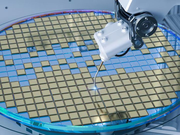
Semiconductor Ceramic Materials: Uses, Types and Trends
Semiconductor ceramic materials support electronic systems through thermal management, electrical insulation, substrates, packaging, and dielectric applications.
Semiconductor ceramic materials are engineered ceramics designed to provide controlled electrical, thermal, mechanical, or dielectric properties in electronic and semiconductor systems. Common families include alumina, aluminum nitride, silicon nitride, zirconia, barium titanate, and other specialized dielectric ceramics.
They exist because modern electronics need more than semiconductor wafers. Chips also require substrates, insulating structures, package components, heat-spreading paths, and reliable electrical connections. Ceramics are useful because many can withstand high temperatures, resist chemical attack, provide electrical insulation, or transfer heat away from sensitive components.
These materials appear in semiconductor packaging, power electronics, RF components, sensors, LED systems, and high-frequency circuits. Their performance depends on purity, grain structure, porosity, dielectric behavior, thermal conductivity, and dimensional stability.
Importance
The importance of semiconductor ceramic materials is increasing as electronic systems become smaller, faster, and more power dense. Artificial intelligence infrastructure, high-performance computing, electric mobility, telecommunications, and industrial electronics all increase the need for materials that manage heat while maintaining electrical isolation.
Different ceramics support different engineering requirements. Alumina is widely used for insulation and substrates. Aluminum nitride is valued for high thermal conductivity with electrical insulation. Silicon nitride can provide strength and thermal stability. Barium titanate is important in dielectric and capacitive applications.
| Material | Common Role | Main Property |
|---|---|---|
| Alumina | Substrates, insulation | Electrical insulation |
| Aluminum nitride | Thermal substrates | High thermal conductivity |
| Silicon nitride | Packaging, structural parts | Strength and stability |
| Barium titanate | Dielectric components | High dielectric constant |
Understanding these differences helps engineers, researchers, and students evaluate ceramic substrate materials, electronic ceramics, advanced dielectric materials, and semiconductor packaging materials.
Recent Updates
U.S. semiconductor policy has placed greater attention on advanced packaging, substrates, and materials. On January 16, 2025, the U.S. Department of Commerce announced $1.4 billion in final awards through the CHIPS National Advanced Packaging Manufacturing Program, including $300 million for advanced substrates and materials research.
On July 29, 2026, Commerce announced letters of intent totaling $874 million for semiconductor research and development covering advanced packaging, substrates, materials, memory, and computing technologies. The announced incentives remained subject to further review and final awards.
On June 17, 2026, Commerce announced a $500 million CHIPS R&D award focused on AI-driven semiconductor materials discovery and approaches for addressing materials bottlenecks and PFAS-related chemistry.
Laws or Policies
In the United States, semiconductor ceramics and related production can be affected by the CHIPS and Science Act, export controls, workplace safety requirements, and environmental rules. The CHIPS framework supports domestic semiconductor manufacturing and research, including advanced packaging and materials development.
Export controls may apply to particular semiconductor technologies, equipment, or related items moving across borders. BIS revised its semiconductor export licensing policy on January 13, 2026. Applicability depends on the item, destination, end user, and end use.
OSHA identifies semiconductor workplace hazards involving chemicals, toxic materials, machinery, and dust, making hazard assessment and appropriate controls important during manufacturing and processing. Environmental requirements may also apply to semiconductor operations, including hazardous air pollutant controls.
Tools and Resources
Helpful learning and analysis resources include:
- Materials databases for thermal conductivity, dielectric constant, density, and strength.
- Phase-diagram tools for composition and temperature behavior.
- Thermal simulation software for heat-flow studies.
- Dielectric measurement equipment for frequency-dependent properties.
- Microscopy and X-ray diffraction for crystal structure and defect analysis.
- Standards databases and technical glossaries for semiconductor materials terminology.
FAQs
What are semiconductor ceramic materials?
They are engineered ceramics used around semiconductor devices for substrates, insulation, packaging, dielectric functions, thermal management, and structural support.
Which ceramic is best for thermal management?
There is no universal choice. Aluminum nitride is widely considered when high thermal conductivity and electrical insulation are both required, while other ceramics may suit different mechanical or dielectric needs.
Are these ceramics themselves semiconductors?
Not necessarily. Many are insulators or dielectric materials used alongside active semiconductor materials.
Why is purity important?
Impurities can change electrical behavior, thermal performance, reliability, and processing consistency. High-purity materials are therefore important in advanced electronics.
What trends are shaping the field?
Key trends include advanced packaging, higher thermal demands, miniaturization, improved metrology, new dielectric systems, and research into alternative chemistries and resilient supply chains.
Conclusion
Semiconductor ceramic materials provide an important supporting foundation for modern electronics. Their thermal, electrical, mechanical, and dielectric properties help address challenges in packaging, power management, insulation, and high-frequency systems. As advanced computing and semiconductor packaging develop, ceramic substrates, thermal materials, and dielectric ceramics are likely to remain important areas of research. Understanding their properties, applications, safety requirements, and policy environment provides a useful foundation for further study.
Disclaimer
This article is for general educational purposes. Material selection, process design, regulatory interpretation, and safety decisions should be based on the specific application, technical specifications, applicable standards, and current U.S. requirements.