PCB Drilling Machines Guide for Precision Circuit Board Manufacturing
Printed circuit boards, commonly known as PCBs, are essential parts of modern electronic products. They provide the physical structure and electrical pathways needed to connect components. As electronic devices become smaller and more powerful, PCB manufacturing requires increasingly precise processes.
One of the most important processes is drilling. PCB drilling machines create holes that support component mounting, electrical connections, and connections between different board layers. The accuracy of these holes can influence the reliability, assembly quality, and electrical performance of the finished circuit board.
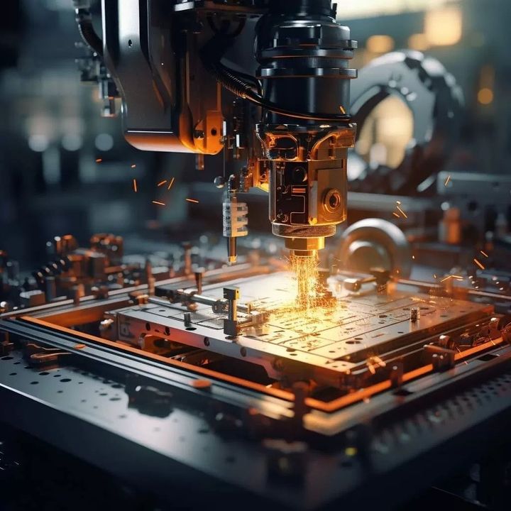
Modern PCB drilling machines combine computer numerical control, high-speed spindles, precision positioning, specialized drill bits, optical alignment, and automated process monitoring. Laser drilling systems are also becoming increasingly important for high-density interconnect, or HDI, boards and very small microvias.
This guide explains PCB drilling machines, their importance, recent developments, applicable policies, and useful resources for understanding precision circuit board manufacturing.
What Are PCB Drilling Machines?
PCB drilling machines are specialized manufacturing systems designed to create controlled holes in printed circuit boards. Depending on the board design, these holes may be used for component leads, plated through-holes, vias, blind vias, or other electrical interconnections.
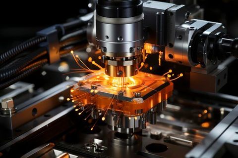
A typical mechanical PCB drilling machine uses a rotating spindle and a small carbide drill bit. The machine follows digital manufacturing data to position the drill at specific coordinates and create holes with controlled diameter and depth.
Laser drilling machines use a focused laser beam instead of a conventional drill bit. They are particularly useful for microvias and HDI applications where very small holes and high positional accuracy are required.
The main types include:
- CNC mechanical drilling machines
- High-speed PCB drilling systems
- Laser drilling machines
- UV laser drilling systems
- CO₂ laser drilling systems
- Hybrid mechanical and laser drilling systems
- Automated multi-spindle drilling systems
The appropriate technology depends on PCB material, layer count, hole diameter, aspect ratio, production requirements, and design complexity.
How PCB Drilling Works
PCB drilling normally takes place after several preparation and lamination stages. The exact manufacturing sequence varies according to board construction.
A simplified process includes:
- Preparing the PCB panel and manufacturing data
- Aligning the panel using reference points
- Selecting appropriate drill tools
- Setting spindle speed and feed parameters
- Drilling programmed hole locations
- Removing dust, debris, and resin smear
- Inspecting hole diameter and position
- Preparing drilled holes for subsequent plating or assembly
For multilayer boards, registration is especially important. A small positional error can cause a drilled hole to miss its intended inner-layer pad.
Drilling parameters also need to match the material. Excessive heat, incorrect feed rates, worn drill bits, or unsuitable drilling conditions can contribute to burrs, resin smear, hole-wall damage, or dimensional variation.
Why PCB Drilling Machines Matter Today
The growing complexity of electronics has increased the importance of precision PCB manufacturing. Smartphones, automotive electronics, communication equipment, industrial controllers, computing hardware, medical electronics, and other systems increasingly depend on compact multilayer circuit boards.
PCB drilling machines help address several manufacturing challenges.
Higher circuit density:
Modern boards often contain many layers and closely spaced electrical connections. Accurate drilling allows designers to use smaller pads and more densely arranged vias.
Reliable electrical connections:
Through-holes and vias provide electrical paths between layers. Consistent hole geometry supports reliable plating and interconnection.
Miniaturization:
Smaller electronic products require smaller circuit boards. Mechanical micro-drilling and laser drilling technologies help accommodate compact layouts.
Manufacturing repeatability:
CNC control allows programmed drilling patterns to be repeated across panels while maintaining consistent positioning.
Production quality:
Automated inspection and process monitoring can identify drilling problems before boards move to later manufacturing stages.
Mechanical Drilling and Laser Drilling Compared
| Feature | Mechanical Drilling | Laser Drilling |
|---|---|---|
| Main tool | Rotating drill bit | Focused laser beam |
| Common use | Through-holes and larger vias | Microvias and HDI structures |
| Tool wear | Requires monitoring | No conventional drill-bit wear |
| Hole size | Suitable for many standard holes | Particularly suitable for very small holes |
| Depth control | Mechanical process | Controlled by laser parameters |
| Typical application | Standard and multilayer PCBs | HDI and advanced circuit structures |
Neither technology is universally better. PCB manufacturers select the method according to board construction, hole geometry, material, and quality requirements.
Recent PCB Drilling Technology Updates
PCB manufacturing continued to move toward greater miniaturization and higher interconnection density during 2025 and 2026.
A major trend is the growing use of HDI manufacturing. HDI boards use fine features and microvias to create dense electrical connections in compact spaces. Laser drilling is particularly relevant because it can form small blind microvias that are difficult to produce using conventional mechanical drilling.
Another important development is the continued refinement of UV and CO₂ laser systems. Different laser wavelengths interact differently with copper, resin, glass-reinforced materials, and other PCB structures. Manufacturers therefore select laser technology according to the material stack and required hole characteristics.
Automation is also becoming more prominent. Modern drilling systems can integrate automatic panel handling, optical alignment, tool management, production data collection, and inspection functions.
At IPC APEX EXPO 2025, held March 18–20, 2025, laser-based PCB micromachining and advanced HDI applications were among the technologies discussed within the electronics manufacturing industry. Industry developments during 2025 and 2026 have continued to emphasize smaller vias, advanced packaging, automation, and precision manufacturing.
Another significant development is the growing electronics manufacturing ecosystem in India. On March 28, 2025, the Union Cabinet approved the Electronics Component Manufacturing Scheme, which was formally notified on April 8, 2025. The initiative aims to strengthen domestic electronics component manufacturing and develop broader supply-chain capabilities.
These developments create a wider environment for advanced PCB fabrication technologies, including precision drilling.
Important PCB Drilling Parameters
Understanding drilling parameters is useful when evaluating PCB manufacturing processes.
Hole diameter:
The required diameter depends on component leads, via structures, plating requirements, and board design.
Spindle speed:
Mechanical drilling uses controlled spindle speeds to achieve suitable cutting conditions. The correct setting depends on tool diameter and material.
Feed rate:
Feed rate influences drilling time, heat generation, hole quality, and tool behavior.
Tool condition:
Drill bits gradually wear during production. Monitoring tool life helps maintain consistent hole dimensions.
Hole position:
Registration accuracy is critical for multilayer boards because drilled holes must align with internal pads and layers.
Aspect ratio:
Aspect ratio compares hole depth with hole diameter. Higher aspect ratios generally require more careful process control.
Debris management:
Drilling creates dust and material debris. Proper extraction and cleaning help maintain process cleanliness.
Laws, Standards, and Policies in India
PCB drilling itself is primarily a manufacturing process, but PCB production facilities may be affected by environmental, waste-management, occupational-safety, and electronics regulations.
The E-Waste (Management) Rules, 2022 came into force on April 1, 2023. These rules establish requirements for specified electrical and electronic equipment and their components, including provisions related to extended producer responsibility and reduction of hazardous substances.
For applicable electronic products, the rules restrict certain hazardous substances, including lead, mercury, cadmium, hexavalent chromium, polybrominated biphenyls, and polybrominated diphenyl ethers, subject to specified concentration limits and applicable provisions.
PCB manufacturing facilities may also need to consider environmental permissions, waste handling, pollution-control requirements, and applicable state-level regulations depending on their processes.
For technical PCB quality, international standards are also important. IPC-2221 provides general printed board design requirements, while IPC-6012F addresses qualification and performance requirements for rigid printed boards. These standards help manufacturers and designers establish appropriate technical expectations for different board constructions.
Organizations working with specialized electronics should verify the latest applicable editions and regulatory requirements before defining production specifications.
Tools and Resources for PCB Drilling
Several general tools can help engineers, designers, students, and manufacturing teams understand PCB drilling.
PCB design software:
Used to create board layouts, define hole locations, specify vias, and prepare manufacturing data.
Gerber and manufacturing-data viewers:
Useful for checking PCB artwork and verifying drill locations before production.
Drill-file analysis tools:
These help review hole sizes, coordinates, tool numbers, and drilling patterns.
PCB design calculators:
Useful for evaluating parameters such as trace geometry, impedance, current capacity, and basic manufacturing constraints.
Tool-life tracking templates:
Spreadsheets can record drill usage, tool changes, hole counts, and inspection results.
Microscope and measurement tools:
Optical inspection equipment can help examine drilled holes, burrs, surface conditions, and registration.
Quality-control checklists:
A structured checklist can cover hole diameter, position, cleanliness, wall condition, and post-drilling inspection.
IPC technical resources:
Industry standards and design guidance can help engineers connect PCB design requirements with manufacturing capabilities.
Common PCB Drilling Problems
Several issues can affect drilling quality.
Hole position errors:
Incorrect panel alignment or registration can shift holes from their intended locations.
Resin smear:
Heat generated during mechanical drilling can soften resin and create deposits on hole walls.
Burr formation:
Improper drilling conditions or worn tools may produce unwanted material around hole openings.
Tool breakage:
Very small drill bits are sensitive to excessive mechanical stress and unsuitable process conditions.
Hole-wall damage:
Incorrect speed, feed, material conditions, or tool selection can affect hole-wall quality.
Laser debris:
Laser drilling may leave residue that requires appropriate cleaning or desmear processes before subsequent operations.
Process monitoring and inspection are therefore important parts of precision PCB manufacturing.
Frequently Asked Questions
What is the main purpose of a PCB drilling machine?
A PCB drilling machine creates controlled holes in printed circuit boards. These holes can support component mounting, electrical connections, vias, and connections between multiple PCB layers.
What is the difference between mechanical and laser PCB drilling?
Mechanical drilling uses rotating drill bits, while laser drilling uses a focused laser beam. Mechanical drilling is widely used for conventional holes, while laser drilling is particularly useful for small microvias and HDI structures.
Why is drilling accuracy important for multilayer PCBs?
Multilayer boards contain electrical layers positioned inside the PCB. A drilled hole must align correctly with its intended internal pad or connection. Poor registration can affect electrical connectivity and manufacturing quality.
What are microvias in PCB manufacturing?
Microvias are very small interconnection structures commonly associated with HDI circuit boards. They connect selected layers and help increase circuit density within compact PCB designs.
Which standards are relevant to PCB manufacturing?
Relevant standards depend on the board type and application. IPC-2221 addresses printed board design, while IPC-6012 provides qualification and performance requirements for rigid printed boards. Additional standards may apply to automotive, medical, aerospace, or other specialized applications.
Conclusion
PCB drilling machines are a fundamental part of modern circuit board manufacturing. They create the holes and interconnections needed to transform PCB designs into functional electronic structures.